
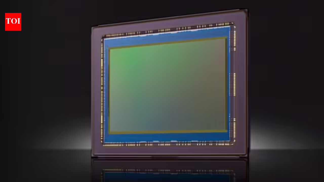
sony and TSMC have signed a memorandum of understanding to form a joint venture developing next-generation image sensors in Japan. The partnership, announced May 8, pairs Sony’s sensor design pedigree with TSMC’s manufacturing firepower—a combination that could reshape the competitive landscape for imaging technology.Sony will hold majority control of the new venture. Development and production lines will be based at Sony’s newly built fab in Koshi City, Kumamoto Prefecture—conveniently close to TSMC’s own Japan facility, which has been running since late 2024. The two companies aren’t strangers: TSMC’s Kumamoto fab already supplies logic chips to Sony on 22/28nm and 12/16nm nodes.The ambition stretches beyond smartphone cameras. Both companies have flagged physical AI applications—think self-driving cars and robotics—as key growth areas where advanced sensing capability is quickly becoming non-negotiable.
This is Sony shedding weight, not just making friends
For Sony CEO Hiroki Totoki, the joint venture is a piece of a much larger puzzle. He’s steering the company toward a “fab-light” model—fewer physical assets, more focus on intellectual property. Sony has already handed its Bravia TV manufacturing to TCL. The chip business is next in line for that treatment.Funding will roll out in phases, contingent on market demand and Japanese government backing. METI has already committed subsidies of up to ¥60 billion—around $380 million—for the Kumamoto facility. Sony is also weighing further investment at its Nagasaki plant.The stakes are real. Samsung has been quietly chipping away at Sony’s grip on Apple’s sensor supply chain, and the pressure is showing. Bringing TSMC into the fold isn’t just a manufacturing upgrade—it’s Sony acknowledging that dominating the next era of image sensors requires a different playbook than the last one.