

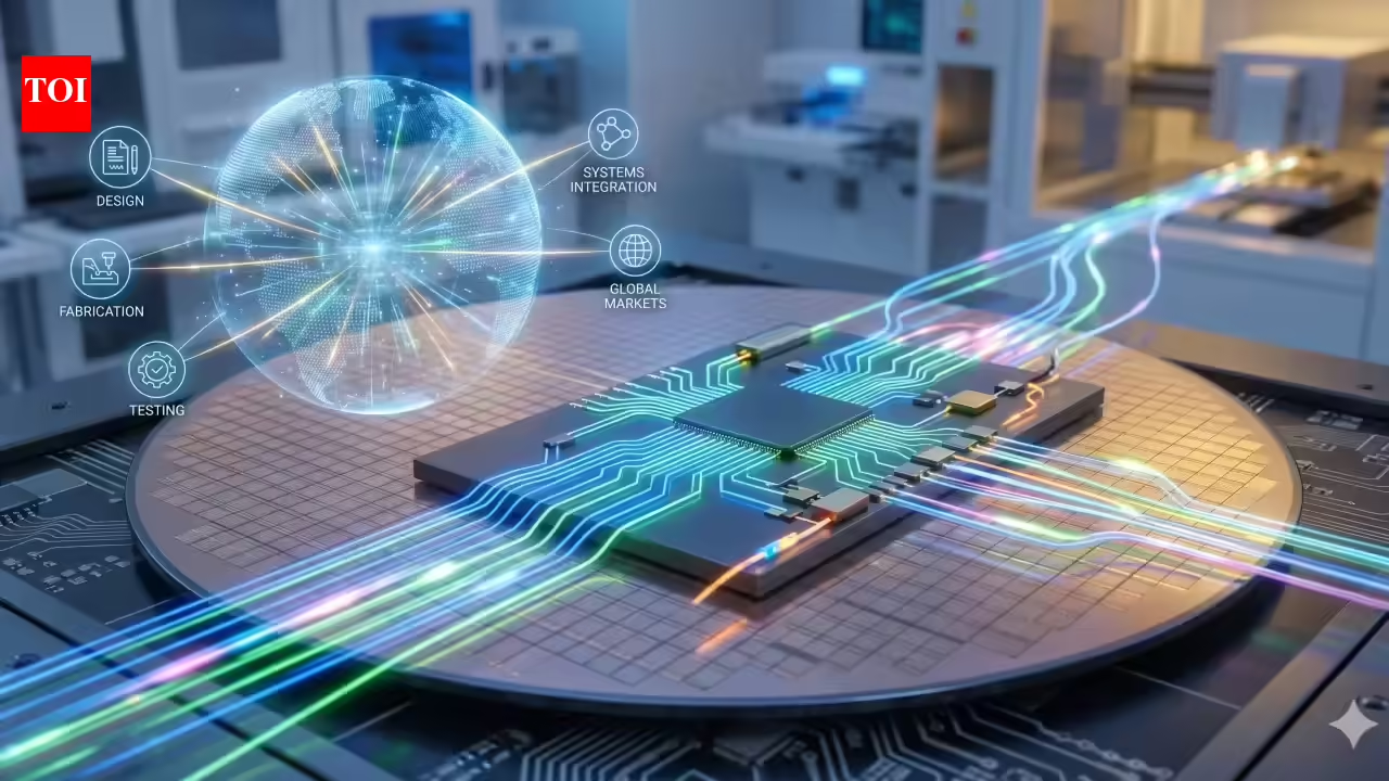

In a push to strengthen India’s semiconductor and photonics ecosystem, indigenously developed silicon photonics technology solutions — including a Process Design Kit (PDK) and a programmable photonic chip test engine — were launched at the Indian Institute of Technology Madras on Friday, marking a key step toward technological self-reliance in advanced chip design.The solutions were unveiled by S Krishnan, secretary at the ministry of electronics and information technology (MeitY), in the presence of Amitesh Sinha, additional secretary at MeitY and CEO of the India Semiconductor Mission, along with senior faculty and governing council members.Developed under the MeitY-supported Center of Excellence for Silicon Photonics at IIT-M, the technologies are expected to function as a shared national facility for industry, startups, academia and defense R&D organizations working on photonic integrated circuits.The silicon photonics PDK — a foundational tool for chip design — comprises over 50 verified components, enabling domestic capability in designing advanced photonic integrated circuits. The universal programmable photonic integrated circuit (PPIC) test engine, meanwhile, is an automated platform designed for characterization of photonic and optoelectronic modules across applications.Calling the development a “major milestone” for India’s technology sovereignty, Krishnan said the country’s capabilities in silicon photonics are now “matching global state of the art”, but stressed the need to complement design advances with manufacturing infrastructure. “This needs to be complemented with establishment of a silicon photonics fab under the India Semiconductor Mission,” he said.Sinha said the technology holds potential across both classical and quantum domains, adding that it could be supported under the proposed ISM 2.0 framework focused on research and development. He indicated that, subject to industry participation and commercial validation, India could move toward setting up a dedicated silicon photonics fabrication facility with integrated packaging capabilities.According to Prof Bijoy Krishna Das, chief investigator of the centre, the next phase will enable multi-project wafer (MPW) fabrication runs from the third quarter of the current financial year, alongside integrated testing, packaging and module characterization services.The center follows a product research, development and manufacturing (PRDM) model based on CMOS-compatible silicon photonics technology, with Malaysia’s SilTerra as the foundry partner and Bengaluru-based izmo Microsystems supporting packaging.The launch comes amid India’s broader push to build domestic capabilities across the semiconductor value chain, with photonics emerging as a critical frontier for high-speed computing, communications and next-generation technologies.